PRODUCTS
Clean Transfer System
Pre-Aligner
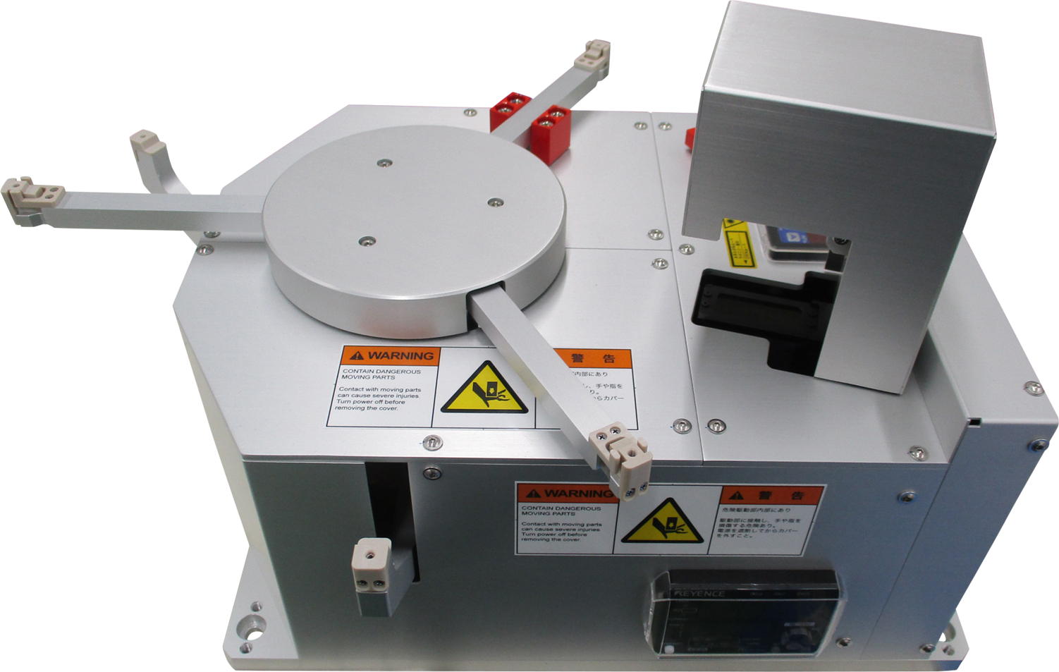
MAF-S Series For Compound Wafer,Glass WaferEdge Hold MAF-SHKZ
This 300mm mechanically clamping wafer aligner minimizes wafer particle contamination by avoiding contact with the backside of the wafer.
Features
###Configurable for compound semiconductor wafers and glass wafers.(Please inquire for details)
###Clean alignment enabled by limiting contact to the wafer edge.
###Notch/Flat are automatically recognized, eliminating the need for host controller settings.
###Built-in controller for a compact design.
Specification
- Wafer handling
- φ300mm SEMI/JEIDA standard wafer.(Please inquire with regard to special wafers such as glass wafers.)
- Alignment time
- 8.0seconds or less(20.0seconds of less when separate chucking required)
- Alignment accuracy
- θ:±0.2° or less(3σ)
- Wafer off-center limit
- ±1mm or less(Wafer offset from chuck center)
- Wafer holding method
- Edge hold
- Wafer detection
- Photo micro sensor
- Communication
- RS-232C(Serial Interface)
- Utility
- Power:DC24V±10% 3A 1lineDry air:φ6mm 0.35MPa to 0.4MPa 1line
- Mass
- Main body:Appox.8kg
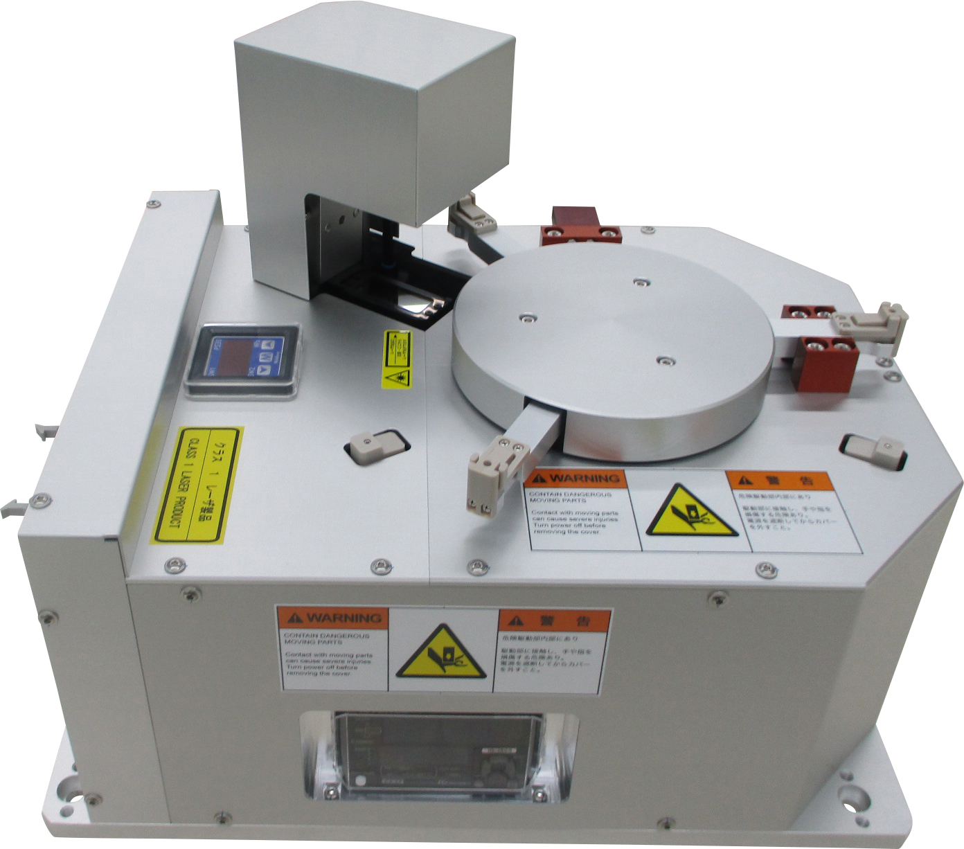
MAF-S Series For Compound Wafer,Glass WaferEdge Hold MAF-SJ
This 200mm mechanically clamping wafer aligner minimizes wafer particle contamination by avoiding contact with the backside of the wafer.
Features
###Configurable for compound semiconductor wafers and glass wafers.(Please inquire us for details)
###Clean alignment enabled by limiting contact to the wafer edge.
###Notch/Flat are automatically recognized, eliminating the need for host controller settings.
###Built-in controller for a compact design.
Specification
- Wafer handling
- φ200mm SEMI/JEIDA standard wafer.
- Alignment time
- 8.5seconds or less(20.0seconds of less when separate chucking required)
- Alignment accuracy
- θ:±0.2° or less(3σ)
- Wafer off-center limit
- ±1mm or less(Wafer offset from chuck center)
- Wafer holding method
- Edge hold
- Wafer detection
- Photo micro sensor
- Communication
- RS-232C(Serial Interface)
- Utility
- Power:DC24V±10% 3A 1lineDry air:φ6mm 0.35MPa to 0.4MPa 1line
- Mass
- Main body:Appox.8kg
MAF-S Series For Compound Wafer,Glass WaferEdge Hold MAF-SK
This 150mm mechanically clamping wafer aligner minimizes wafer particle contamination by avoiding contact with the backside of the wafer.
Features
###Configurable for compound semiconductor wafers and glass wafers.(Please inquire us for details)
###Clean alignment enabled by limiting contact to the wafer edge.
###Notch/Flat are automatically recognized, eliminating the need for host controller settings.
###Built-in controller for a compact design.
Specification
- Wafer handling
- φ150mm SEMI/JEIDA standard wafer.
- Alignment time
- 8.5seconds or less(20.0seconds of less when separate chucking required
- Alignment accuracy
- θ:±0.2° or less(3σ)
- Wafer off-center limit
- ±1mm or less(Wafer offset from chuck center)
- Wafer holding method
- Edge hold
- Wafer detection
- Photo micro sensor
- Communication
- RS-232C(Serial Interface)
- Utility
- Power:DC24V±10% 5A 1lineDry air:φ6mm 0.35MPa to 0.4MPa 1line
- Mass
- Main body:Appox.8kg
Sales Div.Transfer Business Unit
+81-86-239-5117
+81-86-239-5118
