PRODUCTS
Clean Transfer System
Pre-Aligner
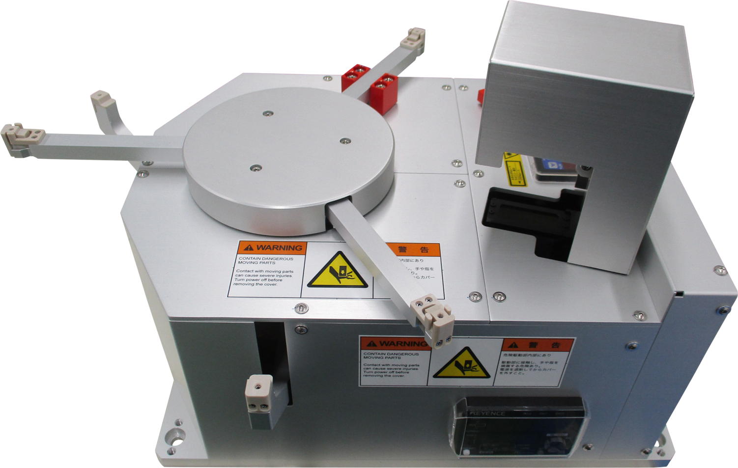
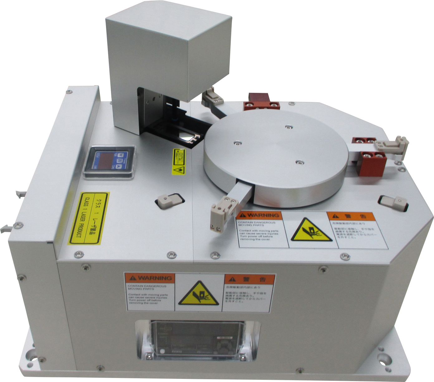
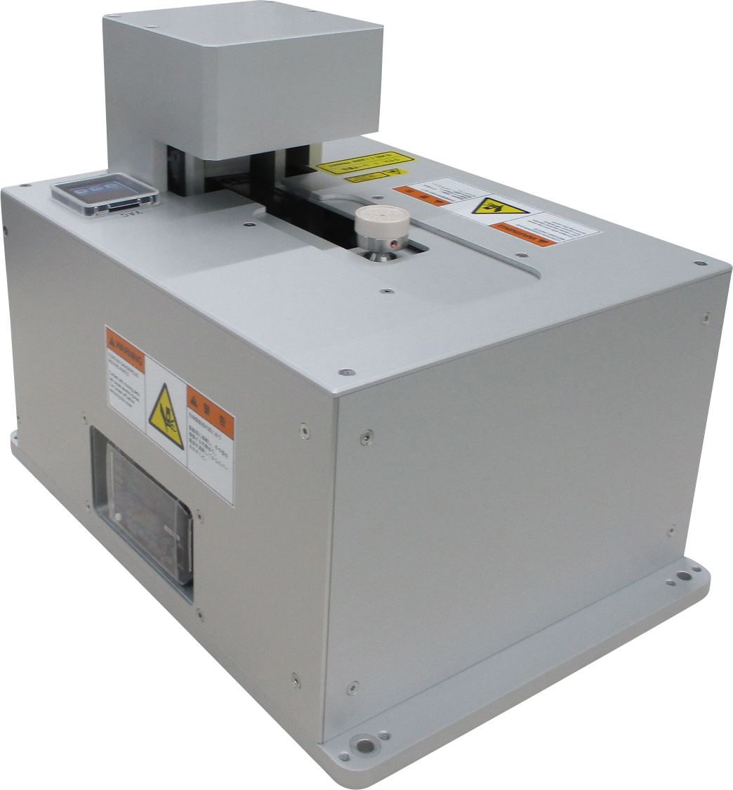
MAF-S Series For Compound Wafer,Glass WaferEdge Hold MAF-SHKZ
This 300mm mechanically clamping wafer aligner minimizes wafer particle contamination by avoiding contact with the backside of the wafer.
Features
###Configurable for compound semiconductor wafers and glass wafers.(Please inquire for details)
###Clean alignment enabled by limiting contact to the wafer edge.
###Notch/Flat are automatically recognized, eliminating the need for host controller settings.
###Built-in controller for a compact design.
Specification
- Wafer handling
- φ300mm SEMI/JEIDA standard wafer.(Please inquire with regard to special wafers such as glass wafers.)
- Alignment time
- 8.0seconds or less(20.0seconds of less when separate chucking required)
- Alignment accuracy
- θ:±0.2° or less(3σ)
- Wafer off-center limit
- ±1mm or less(Wafer offset from chuck center)
- Wafer holding method
- Edge hold
- Wafer detection
- Photo micro sensor
- Communication
- RS-232C(Serial Interface)
- Utility
- Power:DC24V±10% 3A 1lineDry air:φ6mm 0.35MPa to 0.4MPa 1line
- Mass
- Main body:Appox.8kg
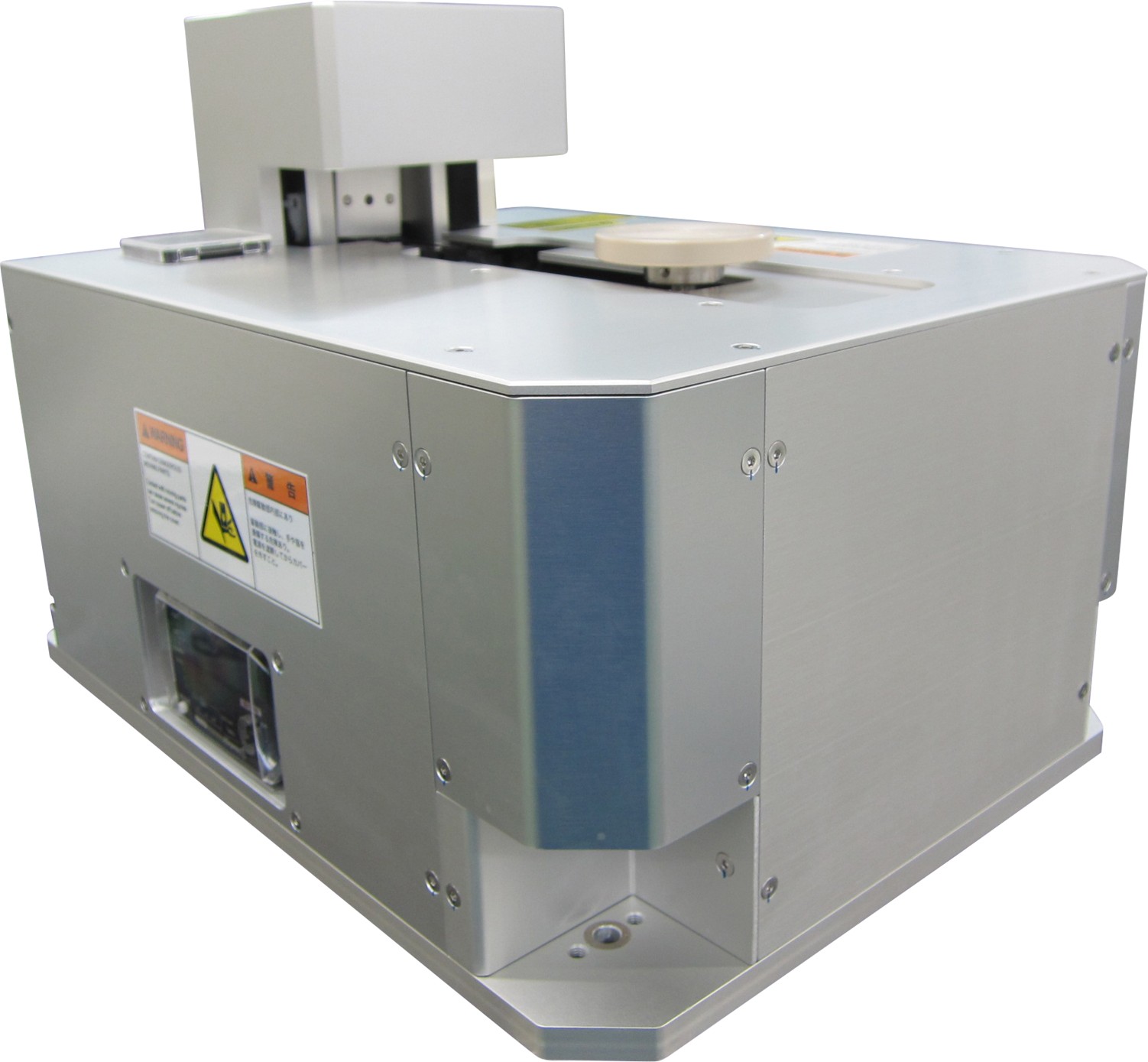
MAF-S Series For Compound Wafer,Glass WaferEdge Hold MAF-SJ
This 200mm mechanically clamping wafer aligner minimizes wafer particle contamination by avoiding contact with the backside of the wafer.
Features
###Configurable for compound semiconductor wafers and glass wafers.(Please inquire us for details)
###Clean alignment enabled by limiting contact to the wafer edge.
###Notch/Flat are automatically recognized, eliminating the need for host controller settings.
###Built-in controller for a compact design.
Specification
- Wafer handling
- φ200mm SEMI/JEIDA standard wafer.
- Alignment time
- 8.5seconds or less(20.0seconds of less when separate chucking required)
- Alignment accuracy
- θ:±0.2° or less(3σ)
- Wafer off-center limit
- ±1mm or less(Wafer offset from chuck center)
- Wafer holding method
- Edge hold
- Wafer detection
- Photo micro sensor
- Communication
- RS-232C(Serial Interface)
- Utility
- Power:DC24V±10% 3A 1lineDry air:φ6mm 0.35MPa to 0.4MPa 1line
- Mass
- Main body:Appox.8kg
MAF-S Series For Compound Wafer,Glass WaferEdge Hold MAF-SK
This 150mm mechanically clamping wafer aligner minimizes wafer particle contamination by avoiding contact with the backside of the wafer.
Features
###Configurable for compound semiconductor wafers and glass wafers.(Please inquire us for details)
###Clean alignment enabled by limiting contact to the wafer edge.
###Notch/Flat are automatically recognized, eliminating the need for host controller settings.
###Built-in controller for a compact design.
Specification
- Wafer handling
- φ150mm SEMI/JEIDA standard wafer.
- Alignment time
- 8.5seconds or less(20.0seconds of less when separate chucking required
- Alignment accuracy
- θ:±0.2° or less(3σ)
- Wafer off-center limit
- ±1mm or less(Wafer offset from chuck center)
- Wafer holding method
- Edge hold
- Wafer detection
- Photo micro sensor
- Communication
- RS-232C(Serial Interface)
- Utility
- Power:DC24V±10% 5A 1lineDry air:φ6mm 0.35MPa to 0.4MPa 1line
- Mass
- Main body:Appox.8kg
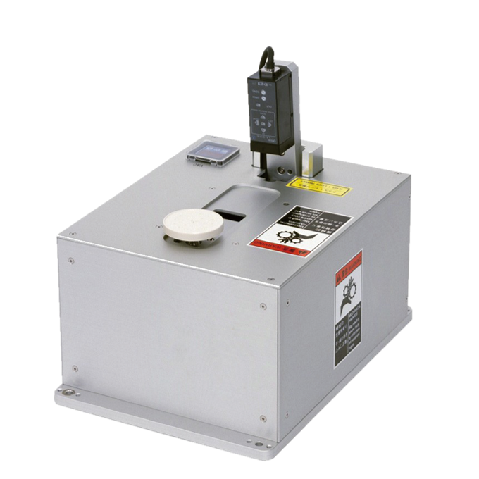
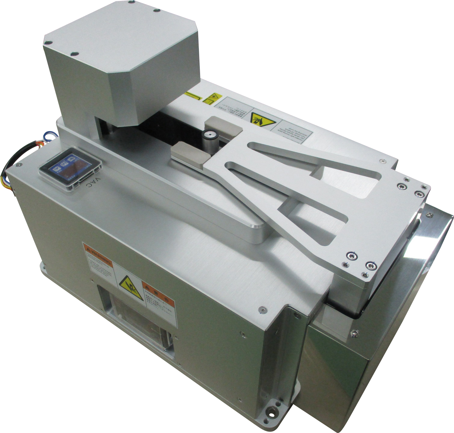
MAF-A Series MAF-AA
This eage contact free unit aligns and centers both flat and notch type wafers at high speeds.
Features
###High speeds are enabled by the units ability to center wafers and perform angle alignment without a seperate chucking.
###Compatible with multiple wafers:200-300mm SEMI/JEIDA silicon wafers.
###Wafer size and nocth/flat are automatically recongnize,eliminating the need for host controller settings.
###Built-in controller for a compact design.
###Controllable through RS-232C or RS-485 serial interface or through photo I/O parallel communications.
Specification
- Wafer handling
- φ200mm to φ300mm SEMI/JEIDA standard wafer.(Please inquire with regard to special wafers.)
- Alignment time
- 3seconds or less(When Processing φ300mm)
- Alignment accuracy
- XY:±0.1mm or less(3σ)θ:±0.1° or less(3σ)
- Wafer off-center limit
- ±5mm or less(Wafer offset from chuck center)
- Wafer holding method
- Backside vacuum chuck
- Wafer detection
- Vacuum sensor with digital display
- Communication
- RS-232C,RS-485(Serial Interface)Photo I/O(Parallel interface)
- Utility
- Power:DC24V±10% 5A 1lineVacuum:-80kPa or less.1line
- Mass
- Main body:Appox.12kg
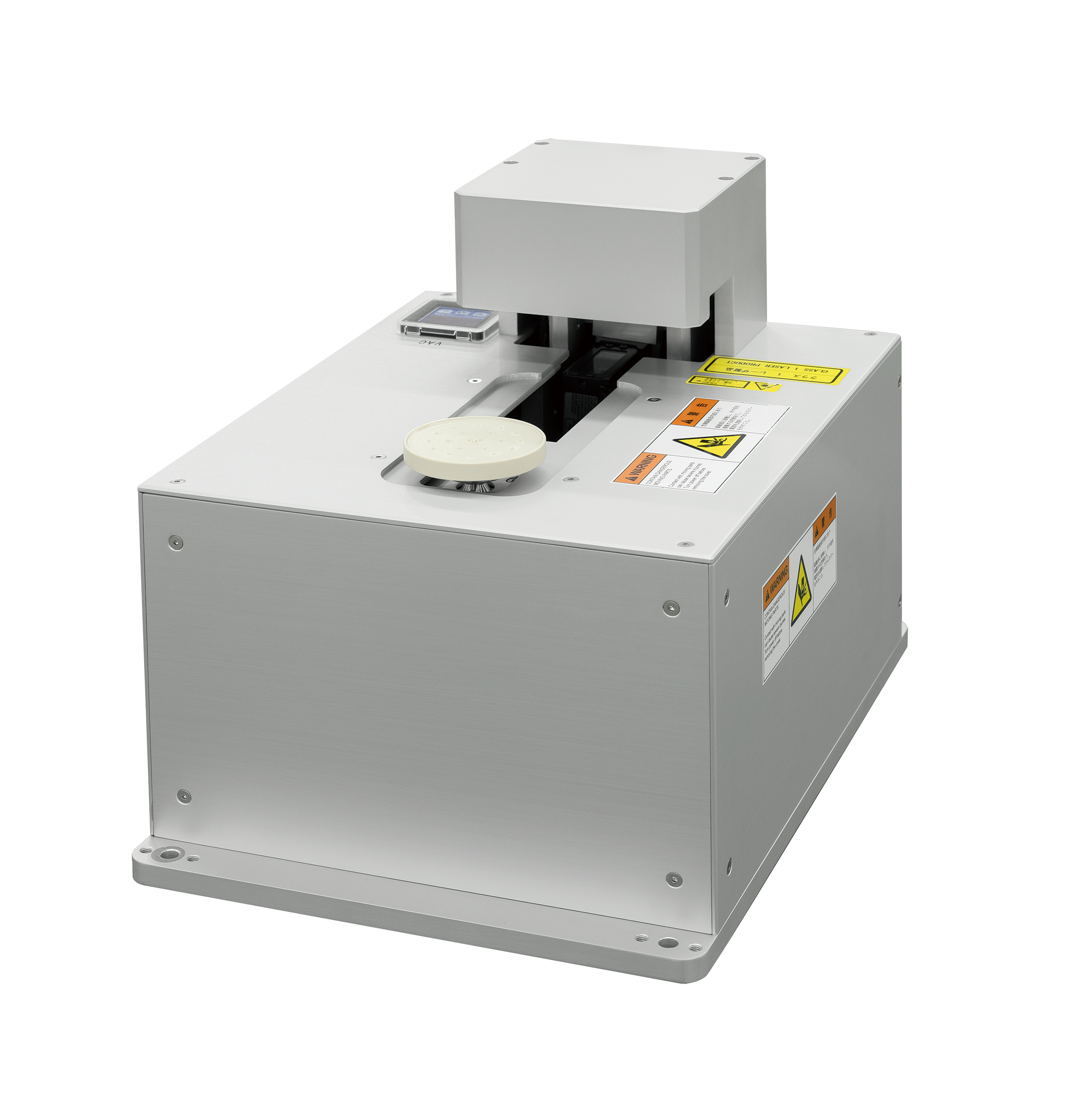
MAF-R Series For Compound Wafer,Glass WaferBackside VAC Chucking MAF-RAPN
This eage contact free unit aligns and centers both flat and notch type wafers at high speeds.
Features
###High speeds are enabled by the units ability to center wafers and perform angle alignment without a seperate chucking.
###Compatible with multiple wafers:200-300mm SEMI/JEIDA silicon wafers.
###Wafer size and nocth/flat are automatically recongnize,eliminating the need for host controller settings.
###Built-in controller for a compact design.
###Controllable through RS-232C or RS-485 serial interface or through photo I/O parallel communications.
###Configurable for compound semiconductor wafers and transparent glass wafers by utilizing CCD photo receiver for line sensor.
Specification
- Wafer handling
- φ200mm to φ300mm SEMI/JEIDA standard wafer.(Please inquire with regard to special wafers such as glass wafers.)
- Alignment time
- 4.5seconds or less(When Processing φ300mm)
- Alignment accuracy
- XY:±0.1mm or less(3σ)θ:±0.1° or less(3σ)
- Wafer off-center limit
- ±5mm or less(Wafer offset from chuck center)
- Wafer holding method
- Backside vacuum chuck
- Wafer detection
- Vacuum sensor with digital display
- Communication
- RS-232C,RS-485(Serial Interface)Photo I/O(Parallel interface)
- Utility
- Power:DC24V±10% 5A 1lineVacuum:-80kPa or less.1line
- Mass
- Main body:Appox.12kg
MAF-RB Series For Compound Wafer,Glass WaferBackside VAC Chucking MAF-RBPN
This eage contact free unit aligns and centers both flat and notch type wafers at high speeds.
Features
###High speeds are enabled by the units ability to center wafers and perform angle alignment without a seperate chucking.
###Compatible with multiple wafers:100-200mm SEMI/JEIDA silicon wafers.
###Wafer size and nocth/flat are automatically recongnize,eliminating the need for host controller settings.
###Built-in controller for a compact design.
###Controllable through RS-232C or RS-485 serial interface or through photo I/O parallel communications.
###Configurable for compound semiconductor wafers and transparent glass wafers by utilizing CCD photo receiver for line sensor.
Specification
- Wafer handling
- φ100mm to φ200mm SEMI/JEIDA standard wafer.(Please inquire with regard to special wafers such as glass wafers.)
- Alignment time
- 5.5seconds or less(When Processing φ200mm)
- Alignment accuracy
- XY:±0.1mm or less(3σ)θ:±0.1° or less(3σ)
- Wafer off-center limit
- ±5mm or less(Wafer offset from chuck center)
- Wafer holding method
- Backside vacuum chuck
- Wafer detection
- Vacuum sensor with digital display
- Communication
- RS-232C,RS-485(Serial Interface)Photo I/O(Parallel interface)
- Utility
- Power:DC24V±10% 5A 1lineVacuum:-80kPa or less.1line
- Mass
- Main body:Appox.12kg
MAF-RC Series For Compound Wafer,Glass WaferBackside VAC Chucking MAF-RC
This eage contact free unit aligns and centers both flat and notch type wafers at high speeds.
Features
###High speeds are enabled by the units ability to center wafers and perform angle alignment without a seperate chucking.
###Compatible with multiple wafers:150-300mm SEMI/JEIDA silicon wafers.
###Wafer size and nocth/flat are automatically recongnize,eliminating the need for host controller settings.
###Built-in controller for a compact design.
###Controllable through RS-232C or RS-485 serial interface or through photo I/O parallel communications.
###Configurable for compound semiconductor wafers and transparent glass wafers by utilizing CCD photo receiver for line sensor.
Specification
- Wafer handling
- φ150mm to φ300mm SEMI/JEIDA standard wafer.(Please inquire with regard to special wafers such as glass wafers.)
- Alignment time
- 4.5seconds or less(When Processing φ300mm)
- Alignment accuracy
- XY:±0.1mm or less(3σ)θ:±0.1° or less(3σ)
- Wafer off-center limit
- ±5mm or less(Wafer offset from chuck center)
- Wafer holding method
- Backside vacuum chuck
- Wafer detection
- Vacuum sensor with digital display
- Communication
- RS-232C,RS-485(Serial Interface)Photo I/O(Parallel interface)
- Utility
- Power:DC24V±10% 5A 1lineVacuum:-80kPa or less.1line
- Mass
- Main body:Appox.12kg
MAF-RP Series For Compound Wafer,Glass WaferBackside VAC Chucking MAF-RP
This eage contact free unit aligns and centers both flat and notch type wafers at high speeds.
Features
###High speeds are enabled by the units ability to center wafers and perform angle alignment without a seperate chucking.
###Compatible with multiple wafers:50.8-100mm SEMI/JEIDA silicon wafers.
###Wafer size and nocth/flat are automatically recongnize,eliminating the need for host controller settings.
###Built-in controller for a compact design.
###Configurable for compound semiconductor wafers and transparent glass wafers by utilizing CCD photo receiver for line sensor.
Specification
- Wafer handling
- φ50.8mm to φ100mm SEMI/JEIDA standard wafer.(Please inquire with regard to special wafers such as glass wafers.)
- Alignment time
- 4.5seconds or less(When Processing φ100mm)
- Alignment accuracy
- XY:±0.2mm or less(3σ)θ:±0.2° or less(3σ)
- Wafer off-center limit
- ±4mm or less(Wafer offset from chuck center)
- Wafer holding method
- Backside vacuum chuck
- Wafer detection
- Vacuum sensor with digital display
- Communication
- RS-232C,RS-485(Serial Interface)Photo I/O(Parallel interface)
- Utility
- Power:DC24V±10% 5A 1lineVacuum:-80kPa or less.1lineDry air:0.4MPa±50kPa 1line
- Mass
- Main body:Appox.14kg
Sales Div.Transfer Business Unit
+81-86-239-5117
+81-86-239-5118
